Article updated on 02 December 2020

25krunya / Shutterstock
Electron microscopy (EM) is a powerful tool in the repertoire of any scientist or researcher, enabling the visualization of samples at the atomic level. As such, it has become a key method in both cell and materials science, owing to the demand for the rapid and detailed visualization of both micro and macromolecules.
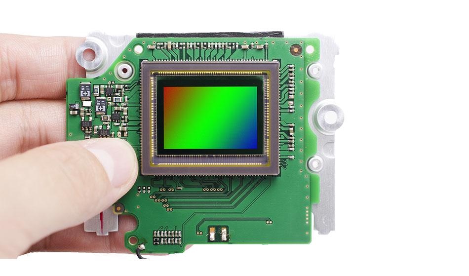
However, any piece of technology undergoes continuous innovation and improvement as compatible technological advances are made. Neither scanning nor transmission electron microscopes are an exception to this, and active pixel detectors potentially represent the most adaptable and advanced option for maximum throughput and image quality in EM.
Innovation
Traditionally, photographic film was the media of choice for capturing EM images, providing both a large active area and adequate sensitivity for image capture. Currently, film is no longer appropriate as many experiments now produce vast quantities of data and require better resolution and speed of image rendering than film can provide.
Throughout the early 2000s, EM technology began to embrace the use of slow-scan charge-coupled devices (CCDs) which were more effective than film but suffered from high levels of radiation sensitivity to the extent that they were unsuitable for working with intermediate voltage electron microscopes. In fact, in order to be utilized in combination with electron microscopes using intermediate voltages (above 100kV), electron deceleration to 100kV was required before the impact of electron to camera to avoid rapid device degradation. In the late 2000s, the invention of direct semiconductor pixel detectors offered a practical solution to these problems.
Pixel Sensors as a Necessity
Pixel sensors came to boast both a greater point spread function, functionally improving depth resolution, as well as a detective quantum efficiency when compared to either CCDs or film. Additionally, both detection and image rendering are much faster with active pixel sensors, enabling a higher throughput approach to EM than what was previously achievable.
Pixel sensors were also a breakthrough innovation in the field of cryo-electron microscopy, in which signal detection technology has limited achievable resolution. Pixel sensors remedy this, with the functional ability to detect single electrons via direct detection systems. In addition to this, pixel sensors have individual lifetimes of several years, reducing expenditure on film and in the case of CCDs, removing the kV limitations placed on researchers, and removing the problem of rapid device degradation when utilized with intermediate voltage electron microscopes.
It should be noted that pixel sensors are under continuous redevelopment and improvement, with current detectors offering pixels of only 2.5 µl, which has allowed improvements in radiation hardness, with thinner oxides. Over time, sensor thinning has reduced the phenomenon of back-scattering, which has led to a better point spread function and thus, a much greater resolution.
A key advantage of active pixel detectors is that single electrons can be detected and visualized by direct detection. It is possible, from this data, to reconstruct larger scale events, and therefore improve resolution in a technique known as “cluster imaging”, which draws parallels to super-resolution microscopy in the form of both confocal and deconvolution microscopes which “break” the resolution limits of non-EM-technology. In cluster imaging, multiple frames will be superimposed against each other to rebuild a more complete image and can be carried out at a lower electron dose.
Like any other field, EM technology improves as time goes by, with innovation and continuous trial and error in modifications. During its antiquity, this came in the form of higher dose electron beams or changes to beam focusing equipment. Now, the durability and effectiveness of image detection technology can make or break an EM system, potentially bypassing the limits of their already impressive resolution and magnification potential.
Sources
- Ruskin, R., Yu, Z. and Grigorieff, N. (2013). Quantitative characterization of electron detectors for transmission electron microscopy. Journal of Structural Biology, 184(3), pp.385-393.
- Downing, K. and Mooney, P. (2008). A charge coupled device camera with electron decelerator for intermediate voltage electron microscopy. Review of Scientific Instruments, 79(4), p.043702.
- Ruskin, R., Yu, Z. and Grigorieff, N. (2013). Quantitative characterization of electron detectors for transmission electron microscopy. Journal of Structural Biology, 184(3), pp.385-393.
Disclaimer: The views expressed here are those of the author expressed in their private capacity and do not necessarily represent the views of AZoM.com Limited T/A AZoNetwork the owner and operator of this website. This disclaimer forms part of the Terms and conditions of use of this website.