Sponsored by SEMIJul 6 2018
At this year’s SEMICON West, the Advanced Lithography TechXPOT will look at development in extreme ultraviolet lithography (EUVL), its economic viability for high-volume manufacturing (HVM) and other lithography solutions that will enable the march toward 5 nm and further to 3 nm.
.jpg)
Role of Directed Self Assembly in 3 nm
As an introduction to the event, SEMI asked Mary Ann Hockey, director for Advanced & Emerging Lithography at Brewer Science Inc., as well as a speaker at the TechXPOT, to present her knowledge of the status of directed self-assembly (DSA) as it is applicable to the industry’s march toward patterning for the 3-nm node and further.

Mary Ann Hockey, director for Advanced & Emerging Lithography at Brewer Science Inc.
SEMI: What is the present status of materials development for DSA?
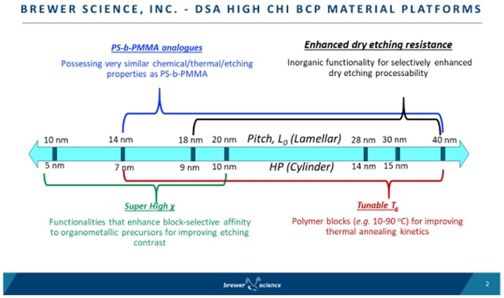
Hockey: At present, the company is working with strategic customers to execute high-quality DSA chemical material solutions. It is focusing on near-term implementation of standard PS-b-PMMA block copolymers (28-30 nm Lo) by exploiting its strategic collaboration with Arkema, France, and developing an archive of high-chi block copolymers for long-term device requirements (Figure 1).

Figure 1. DSA high-chi block BCP material platforms. (Source: Brewer Science Inc.)
SEMI: How do those developments groom the technology for 5 nm, 3 nm, or beyond?
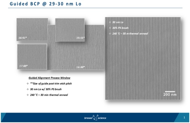
Hockey: The company has employed the approach of creating an archive of innovative high-chi block copolymer (BCP) platforms for next-generation DSA technology requirements of 3–5 nm devices. A global focus on easing implementation into a manufacturing environment is one of the main goals. Achieving this goal requires large process windows for guided alignment (adapting for pitch and guide size target variability), reducing BCP microphase anneal times (short anneal time promotes high throughput), and streamlining the total number of process steps needed for volume production (Figure 2).

Figure 2. Guided BCP @ 29-30 nm Lo. (Source: Brewer Science Inc.)
SEMI: How will industry’s use of DSA be entwined with immersion lithography?
Hockey: The company visualizes immersion lithography as the base enabler with strategic application of optical lithography for producing consistent critical dimension (CD) sizes of DSA guides/templates for cost-effective ownership.
SEMI: What about the combination of extreme ultraviolet lithography (EUVL) and DSA to fabricate devices at 5 nm, 3 nm, and beyond?
Hockey: EUVL and DSA have the capacity to work in tandem to support next-generation device technology. It is possible to craft DSA with the capability of lithography rectification or improving EUVL photoresist sidewalls and targeting low line-width roughness and line-edge roughness (LWR/LER) values.

This information has been sourced, reviewed and adapted from materials provided by SEMI.
For more information on this source, please visit SEMI.