The development of highly-integrated and cost-effective circuits for future radar and imaging systems is enabled with the monolithic integration of RF-MEMS into a SiGe-BiCMOS technology. Likewise, the development of high performing, reliable RF-MEMS switches has been enabled by Laser Doppler vibrometry (LDV) and coherence scanning interferometry (WLI).
Bicmos RF-MEMS Switch Integration
For mm-wave applications such as WLAN, radar and imaging, SiGe-BiCMOS technologies are becoming increasingly interesting. Reconfigurable integrated circuits (IC) are frequently required for these applications. RF-MEMS along with their improved RF-performance are beneficial for different frequency bands, signal path switches between transmitter, receiver and antenna as well as phased-array systems (Figure 1).
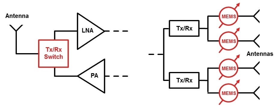
Figure 1: RF-MEMS switch used as Tx/Rx-switch (left) or phaseshifter (right).
As shown in Figure 2, the capacitive-type RF-MEMS switch is monolithically integrated into the backend-of-line (BEOL) of IHPs SiGe-BiCMOS technology, enabling the shortest interconnections between transistors and MEMS. This then prevents, or at the very least, minimizes high-frequency parasitic effects.
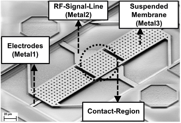
Figure 2: Scanning electron microscopy picture of RF-MEMS switch.
The first three BEOL metallization layers execute the switch. Metal 1 produces the high-voltage electrodes for electrostatic actuation., Metal 2 is used as the RF-signal line. Metal 3 locates the suspended membrane. The membrane position can be modified by applying a voltage to the electrodes. This changes the capacitive coupling between the signal line and suspended membrane, which in turn leads to efficient switching of high-frequency signals.
Experimental Setup
Several methods for mechanical, electrical and RF-characterization are required for the development of RF-MEMS switches. Electromechanical performance is crucial because RF-performance is strongly influenced by it. Optical characterization techniques are preferred because highest resolution measurements are possible with zero influence on the behavior of the device.
Automated 200 mm wafer-level electromechanical motion characterization of the RF-MEMS switches is carried out using the MSA-500’s LDV, and static deformation is analyzed with WLI . The ability to detect “out-of-plane” motions with nm- range displacement resolution and µm spatial resolution makes LDV an outstanding measurement method for process-control.
Results
Parameters such as pull-in voltage and switching-time can be extracted by applying different actuation voltages. The RF-MEMS switch technology demonstrated in Figure 3 can achieve excellent uniformity.
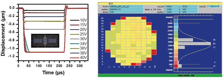
Figure 3: LDV-measurement shows membrane displacement with different actuation voltages (left) and waferlevel homogenity (right).
The membrane displacement enables conclusions to be drawn on the mechanical spring constant and the influence of residual stress. The mechanical, electrical and RF-performance is significantly influenced by residual stress and, as such, requires regular detection (Figure 4).
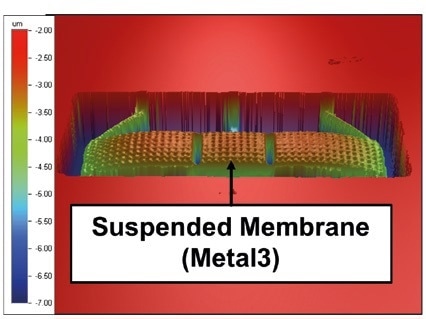
Figure 4: WLI of an RF-MEMS switch shows the influence of residual stress inside the thin layers.
Charging and fatigue can lead to device failure meaning that a major obstacle for the successful application of RF-MEMS is reliability. Several switches can be tested in parallel with LDV, making it useful for reliability detection and in turn, design improvement. Over billions of switching cycles, the ability to test in parallel enables a fast and very cost-effective analysis (Figure 5).
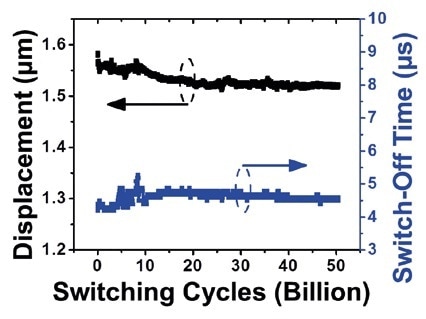
Figure 5: RF-MEMS switch reliability test using LDV.
Conclusion and Outlook
The monolithic integration of RF-MEMS switches has progressed in recent years in terms of performance, process stability, yield and reliability, . This is in part due to the application of LDV and WLI. Fast and cost-efficient detection of electromechanical performance at the wafer-level are enabled by these characterization methods for the development of reliable mm- wave systems. The recently developed intelligent antenna-array with integrated RF-MEMS switches is one example of this (Figure 6).
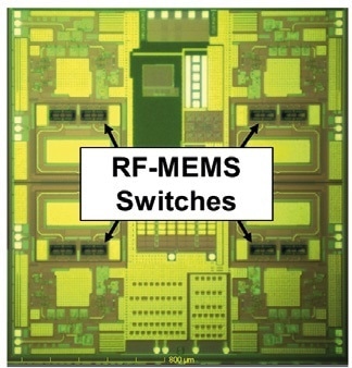
Figure 6: Transceiver quad-chip for intelligent antenna-arrays.

This information has been sourced, reviewed and adapted from materials provided by Polytec.
For more information on this source, please visit Polytec.