AZoSensors speaks with Kaylee Hakkel from MantiSpectra, a vertically-integrated spin-off of the Eindhoven University of Technology, about her research into developing a near-infrared sensor that dramatically simplifies spectral sensing.
What inspired your research into developing a near-infrared sensor that is comparable in size to smartphone sensors?
There is nothing more exciting than being able to sense the world that is all around us. How useful would it be if we could use a sensor to determine if the food in our fridge is still okay even though it is past its expiration date? Besides the application side, scaling down a commonly used instrument also brings exciting physics and engineering-based challenges.
In what applications is spectral sensing typically used?
Spectral sensing is used to quantify and classify materials in a broad range of application fields. Spectroscopy/spectral sensing is used in the fields of medicine, physics, chemistry and astronomy. The technique is used in research, industry, agriculture, healthcare and many more fields.
However, to commercialize this technique for the portable consumer, it is essential to have a cheap and scaled-down instrument.
What are some of the setbacks of current near-infrared spectrometers?
The problem with the current solutions is that they are quite often too big to make into a portable solution or too expensive to make it available for a broad range of applications. There are cheap portable solutions already available in the visible wavelength range by making use of the well-matured Silicon technology. However, to expand this to the near-infrared range, it is more expensive.
How does your near-infrared sensor overcome the aforementioned drawbacks of conventional near-infrared spectrometers?
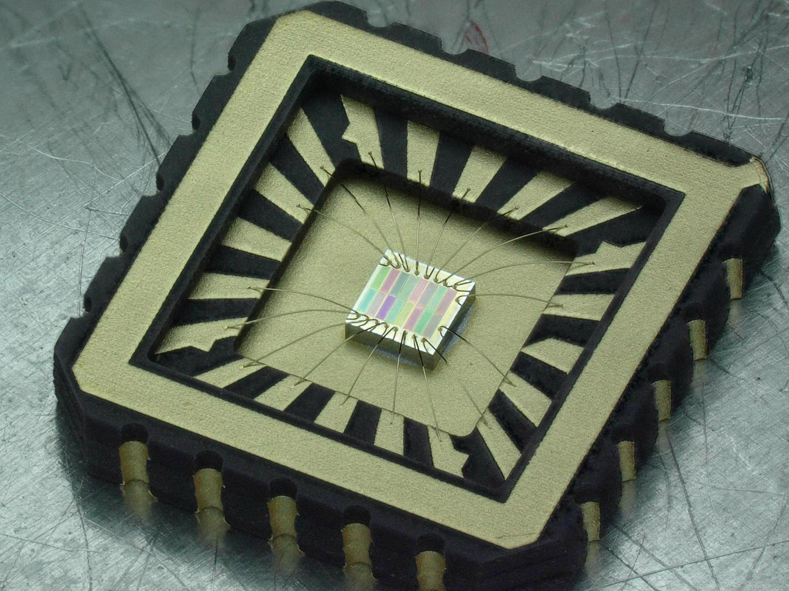
We have developed a spectral sensing chip that can be fabricated on a wafer scale level. This means that the sensor is very small and is also cheap to fabricate since the fabrication can be easily scaled up.

We also make use of a rigid sensor design that does not include any moving elements as is, for example, the case in MEMS-based solutions. This makes the fabrication process easier, but besides that, it also provides a solution that is more suitable for portable applications where the sensor will be constantly moved around.
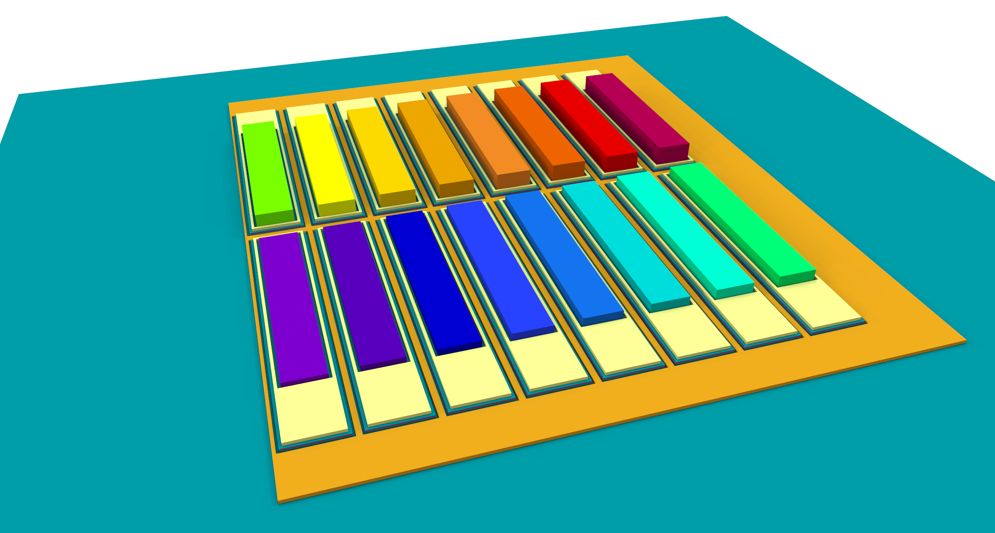
As we make use of 16 pixels, we can get all the spectral information across the NIR range (850-1700 nm) in a single shot measurement. This is because all pixels have an optical response that is not only at a single wavelength.
Your sensor has got 16 different sensors that are all sensitive in the near-infrared. What inspired this?
We found the inspiration for our spectral sensor in nature. Starting with our eyes, we can sense the world that is all around us using just the three different cones (red, green and blue).

We can, for example, see that a red strawberry is ripe, but a green one is not. It is also important to realize that we do not analyze the spectrum of the objects we are looking at, just the certain color.
However, we are not the only ones with exciting viewing systems, as way more advanced viewing systems exist, for example, the ones of the Mantis shrimp. This creature can have up to 16 different photoreceptors which are not only sensitive in the visible range but also extend into the infrared.
We have seen that for spectral sensing applications, it is beneficial to work in the near-infrared wavelength range because it can provide higher sensitivity for a broad range of organic and inorganic materials as compared to the visible range.
Did you come across any challenges during your research, and if so, how did you overcome them?
The most difficult part was making a sensor design that was robust and, at the same time, easy to fabricate.
One very important thing that we realized was that we needed to get away from the standard method for spectral sensing. In the standard method, you actually use the output values of your spectral sensor to reconstruct the spectrum of the material you are investigating. Then these spectra are used to build a prediction model.
However, we saw that we did not need this intermediate step of spectral reconstruction in order to have a properly working prediction model.
So, instead, we use the output values of our spectral sensor directly as input for the prediction model. In that way, we do not need to make any assumptions on the to be reconstructed spectra, but most importantly, it strongly simplifies the integration of the sensor on a chip.
Using this approach we, for example, do not need to have an optical response of a single pixel that has just a single peak wavelength value. This means that the spectral response of a single pixel can have multiple wavelength peaks. The output values of all pixels combined are then directly used for the prediction model.
How does your novel approach compare to traditional means of using sensors to measure light?
The main difference between our novel approach and conventional means is that we have robust sensors consisting of 16 pixels. These pixels all have a spectral response that does not represent a single wavelength. The output values of the pixels are directly used in the prediction model. This means that no spectral reconstruction is used.
How did you test the efficacy of the sensor, and what were the results of your experiments?
In the Nature Communications article, we show the use of our sensor for several application cases. For us, it was important to show that we can use our sensor in these relevant application cases instead of just showing the optical properties.
Our sensor has, for example, been used for the determination of the nutritional properties of milk. This can give great insights to the farmers which helps to select the right feed and monitor the cow’s health or the quality of the milk. In the article, we also show its application in the classification of different plastic types.
What are the potential applications of this sensor, and what impact will such a device have on industry?
Scaling down the size of spectral sensors and making them easy to fabricate is key for the industry. We integrate the full spectral sensing on a chip that can be fabricated at the wafer level. This strongly reduces the cost and therefore enables its use in a broad range of applications. For example, distributed sensors for quality measurements, material identification in process-control and agriculture or portable scanners.
The sensor can be employed directly where needed: on the field by farmers, in the process line on conveyor belts, along the full production chain, at the point-of-care.
MantiSpectra is already helping farmers to monitor the sugar and ripeness level of tomatoes during their growth without destroying the fruit. The same data can be used to determine grade and shelf-life after harvesting.
The sensor can also be used in a circular economy where the recycling of products is important. The sensor can be used to identify, for example, different plastic and textile types, opening the way for a new era for recycling that makes use of near-infrared analysis.
Besides this, there are many more applications fields, such as the identification of raw materials like the composition of solids, powders and liquids, or the determination of moisture content.
When will this technology be commercially available?
The technology is currently commercialized at MantiSpectra. MantiSpectra, a vertically-integrated spin-off of the Eindhoven University of Technology, is bringing these miniaturized spectral sensors to the market. At MantiSpectra, we believe that integrating spectroscopy at a wafer level will open up new applications where volume, robustness, ease-of-integration are key.
These sensors will be employed directly where needed: on the field by farmers, in the process line on conveyor belts, along the full production chain, at the point-of-care, for recycling, ect.
What are the next steps for your research to advance the sensor?
An important next step is the extension of the wavelength region. Besides that, it is also important to show the use of our sensor in a broader range of application fields.
About Kaylee Hakkel
 Kaylee Hakkel obtained her bachelor’s degree in Applied Physics in 2015, whereafter she continued with her master’s studies in Applied Physics with a specialization in Bio/Nanoscience and Technology. During her master’s degree, she joined the Photonics and Semiconductor Nanophysics group for her final research project on fiber-tip sensors, which she finalized in 2017. After this, Kaylee started her Ph.D. project on spectral sensors in the same research group. Currently, Kaylee is working as Operations Director at MantiSpectra, a company working on the next generation of spectral sensors.
Disclaimer: The views expressed here are those of the interviewee and do not necessarily represent the views of AZoM.com Limited (T/A) AZoNetwork, the owner and operator of this website. This disclaimer forms part of the Terms and Conditions of use of this website.