Mar 26 2010
The new MS320C5515 Fingerprint Development Kit will be soon launched by Texas Instruments Incorporated (TI).
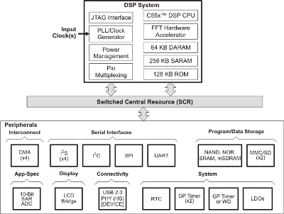
 Functional Block Diagram for TMS320C5515 DSP
The kit offers an entire signal chain solution to integrate fingerprint biometric features in lesser time to market. Incorporating a core board having popular swipe and optical sensors and the C5515 digital signal processor (DSP) of TI, the powerful kit also has optimized application software to simplify product development and implementation. This kit will significantly lessen the product design cycle to the extent of 9 to 12 months even for those customers who are not conversant with fingerprint application development.
The kit enables precise and speedy matching of fingerprints by leveraging the ability of the DSP platform to carry out important functions in the fingerprint algorithm like transforming, sorting, and filtering. The C5515 kit features the least power 16-bit based fixed point DSP in the industry. This feature enables the kit to offer optimal processing performance even at a low 0.15 mW/MHz power level, resulting in increased battery life for light-weight end equipment. A range of portable applications can be developed by using this kit, such as storage device, USB smart keys, and physical access control products (safe boxes and electronic door locks).
The kit includes a core board with low power C5515 DSP of TI, an extension board with sound indicators, USB 2.0 and RS232 ports for communication with PCs LED, and a power supply circuitry; AuthenTec swipe sensor ATW310 and optical sensor.
The AuthenTec ATW310, a fingerprint sensor with a small form factor, has the memory efficiency and power required for quick recognition of fingerprints to meet requirements of modern-day access control and mobile devices.
Users of the kit will be able to analyze final product performance by using the .out file along with production quality demo. A fingerprint-matching algorithm that runs on the C5515 powers the demo. The C5515 is optimized for recognizing fingerprints within a second and has a less than .0015% rate of false acceptance rate (FAR) and less than 1% false rejection rate (FRR) for ensuring reliability of the system. Even new users can understand the way a new product is developed with fingerprint features by using the simplified application source code.
Along with the kit, technical documents like application notes and user guide, and hardware design collateral with Gerber files and schematics, are also provided for users.
The 70mm × 30mm extension board and the 30mm × 30mm core board enable the kit to have a small form factor solution that meets requirements of portable applications. The architecture with two boards offers more design flexibility, enabling customers to reutilize their designs for developing product lines that are scalable.
The TMS320C5515 DSP has several important features and advantages. Its structure ensures lower power consumption and code execution efficiency by three main techniques. These are enhanced DSP addressing features, using simultaneous multiple access to facilitate increased bandwidth for on-chip memory, and increased parallelism through the dual multiply-accumulate (MAC) units.
The battery life in portable devices is maximized due to elaborate power management features like real-time clock (RTC) only mode, clock gating, and memory retention. It is possible to develop new applications and reduce system costs due to on-chip memory of 320 KB. On-chip low-dropout regulators (LDO), namely, GPIOs, UART, and SPI, and high-speed USB 2.0 form the highly integrated peripherals that also have a role in new applications development.