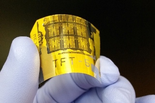
Electrical engineers at University of Wisconsin-Madison have developed a unique, flexible phototransistor that is considered to be the most responsive and fastest silicon phototransistor yet.
 Developed by UW-Madison electrical engineers, this unique phototransistor is flexible, yet faster and more responsive than any similar phototransistor in the world. Credit: Jung-Hun Seo
Zhenqiang "Jack" Ma, professor of electrical and computer engineering, and Jung-Hun Seo, a research scientist, collaborated in this study. Their transistor demonstrates better response time and sensitivity than existing phototransistors.
The new phototransistor holds promise for a wide range of applications that are dependent upon electronic light sensors. Possible applications include digital cameras, satellites, smoke detectors, night-vision goggles, and surveillance systems. In digital camera lens applications, the innovative phototransistor could help increase the quality and acquisition speed of still photos and videos, while reducing the bulkiness of the device.
Phototransistors work in a manner similar to human eyes. They sense light, and then convert it into an electrical charge that is proportional to the wavelength and intensity of the light. In digital cameras, the electrical charge is converted into 0s and 1s, which are then used to generate the digital image. Conversely, in the human eye, the image is transmitted in the form of electrical impulses to the brain.
The innovative phototransistor is flexible, which helps it to better reproduce the behavior of mammalian eyes. Conversely, most other phototransistors developed before now have been flat due to the use of rigid surfaces for their fabrication.
"We actually can make the curve any shape we like to fit the optical system," Ma says. "Currently, there's no easy way to do that."
The researchers employed an innovative "flip-transfer" fabrication method, where the finished phototransistor is inverted onto a plastic substrate in the final step. This leads to a reflective metal layer on the bottom.
"In this structure -- unlike other photodetectors -- light absorption in an ultrathin silicon layer can be much more efficient because light is not blocked by any metal layers or other materials," Ma says.
Electrodes were also placed below the ultrathin silicon nanomembrane layer of the phototransistor. The electrodes and the metal layer function as reflectors, and enhance the absorption of light without the necessity for an external amplifier.
"There's a built-in capability to sense weak light," Ma says. They enable new possibilities, he added.
"This demonstration shows great potential in high-performance and flexible photodetection systems," says Ma, whose work was supported by the U.S. Air Force. "It shows the capabilities of high-sensitivity photodetection and stable performance under bending conditions, which have never been achieved at the same time."
The innovative technology is being patented by the researchers through the Wisconsin Alumni Research Foundation.
The study paper has been published in the journal Advanced Optical Materials.