"While we think of diamonds as very expensive jewelry, they can actually be made using methane and hydrogen. Diamonds are really just carbon, a light and simple element. Their simple yet unique characteristics create significant potential for use in a wide range of purposes, including generation of environmental energy and biological applications," says Professor Mutsuko Hatano.
Diamonds, although nonconductive, can be altered to function as semiconductors with the addition of phosphorus and boron. Silicon, the most common semiconductor, is widely used in memory devices and microprocessors. It is also used in power devices. As power devices are key for social infrastructure that facilitates smart grids, high capacity is required. As a result, the demand for high-capacity power production with minimal loss during power conversion calls for the development of new semiconductor materials.
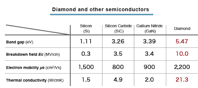
The thermal conductivity of diamonds is 14 times greater than that of silicon, and electrical field resistance is 30 times greater. High thermal conductivity allows the release of heat, which can reduce the size of cooling systems normally required during the generation of increased levels of electric power. High electrical field resistance suppresses power conversion losses. With these characteristics, diamonds are the ultimate semiconductors for electronic devices that require several kilovolts (kV) of power, such as those used in electric vehicles, railways, and power transmission.

Although the formation of diamond-based n-type semiconductors, whose conduction carriers are electrons, and p-type semiconductors, whose conduction carriers are electron holes, has been achieved, the difficulty has traditionally lain in the formation of the lateral p-n junction, which is the basic structure of devices. Collaborating with researchers at the National Institute of Advanced Industrial Science and Technology, Hatano established a lateral p-n junction, which was then applied to a junction field effect transistor (FET) prototype. This was the world's first high-voltage power device, whose application to power supply optimization in smart grids is significantly reducing environmental impact.
Diamond sensor with high potential for biological applications
Hatano is now focusing on the development of a diamond sensor, which has attracted attention around the world due to its potential application to biology.
In a diamond crystal, carbon atoms can be replaced by nitrogen atoms to create nitrogen-vacancy complexes (NV centers). Negatively charged NV centers exhibit a magnetic property called electron spin*. Green light radiation causes the emission of red fluorescence. Depending on the magnetic field, fluorescence processes change, and magnetic field strength and direction can be detected. Diamond sensors apply these characteristics, and the imaging of a magnetic field is enabled.
Diamond sensors are superior to other sensors because they allow a wider range of spatial resolution — from nanometers to millimeters — and have a high magnetic sensitivity. Another outstanding characteristic is that while SQUID magnetic sensors conventionally require a low temperature, diamond sensors operate at room temperature.
Diamond sensors enable scalable application to spatial resolution, which is required for the nanometer-level analysis of protein structures, submicron cell measurement applied to drug delivery and immunological testing, and micron-level analysis of medical imaging, medicines, foods, and noninvasive measurement.