Nov 17 2017
Image sensors that have unmatched resolution and sensitivity to light can be developed by stacking blue-sensitive, red-sensitive, and green-sensitive color sensors on top of one other in place of lining them up in a mosaic form.
Yet, thus far, this has not been achievable. At present, scientists from Empa and ETH Zurich have created a sensor prototype with the ability to absorb light in an almost optimal manner, which is also inexpensive to make.
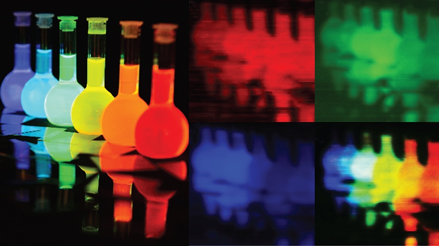
 Original image (left) and corresponding portrayal of the red, green and blue regions, and a composite image. CREDIT: Empa.
There are three distinct types of sensory cells in the human eye for perceiving color. These cells, which are respectively sensitive to blue, green, and red, alternate in the eye and merge their information to develop a comprehensive colored image. Image sensors in mobile phone cameras function in a similar manner: green, blue, and red sensors alternate in a mosaic form. Smart software algorithms have the potential to compute a high-resolution color image from the individual pixels of color.
Yet, the method also has certain intrinsic restrictions—due to the fact each individual pixel of color can absorb only a trivial portion of the light spectrum irradiated on it, a large portion is lost. Moreover, the sensors cannot be miniaturized any further and hence undesired image disturbances, called colour moiré effects, can occur and must be eliminated from the finished image through a laborious process.
Transparent only for certain colors
Hence, scientists have been working for many years on the concept of stacking the three sensors in the place of positioning them in a mosaic form. Naturally, this mandates that the sensor located on top has to allow light frequencies not absorbed by it to the sensor below. During the late 1990s, for the first time researchers successfully produced this type of sensor. It comprised three silicon layers stacked on top of each, where each layer absorbed just one color.
This originally resulted in a commercially accessible image sensor. Yet, it could not be translated into industrial production as the absorption spectra of the individual layers were not adequately different, and hence the blue-sensitive layer absorbed a portion of the red and green light. Therefore, the colors blurred and the light sensitivity was lowered when compared to the normal light sensors. Furthermore, the process for producing the absorbing silicon layers was expensive and complex.
At present, scientists from Empa have been successful in creating a sensor prototype that overcomes these challenges. It comprises of three kinds of perovskites, which are semiconducting materials that have gained a lot of attention in recent years, especially in the making new solar cells, as they have exceptional electrical characteristics and better optical absorption capabilities. Depending on their composition, these perovskites can, for instance, absorb a portion of the light spectrum but can stay transparent for the remaining spectrum. The scientists in Maksym Kovalenko’s team at Empa and ETH Zurich adopted this concept to develop a color sensor that had a size of only one pixel. The team could reproduce simple one-dimensional as well as more realistic two-dimensional images with exceptionally high color fidelity.
Accurate recognition of colors
The benefits of this innovative technology are straightforward—the absorption spectra are clearly distinguished and hence the color recognition is even more accurate than with silicon. Moreover, the absorption coefficients, specifically for the light components that have greater wavelengths, or green and red components, are much higher in the perovskites when compared to silicon. Consequently, the layers can be made considerably smaller, thereby enabling smaller pixel sizes. Considering ordinary camera sensors, this is not very significant, but in the case of other analysis techniques (e.g. spectroscopy), this can enable considerably higher spatial resolution. There is also a relatively inexpensive method for producing perovskites.
Yet, further research is necessary to develop this prototype into a commercially workable image sensor. Important areas of concern are the miniaturization of pixels and the development of techniques for synthesizing a complete matrix of these pixels in a single step. Kovalenko is confident that this can be achieved with exisitng technologies.