British electronics company, Nanusens, has opened a new funding round on CrowdCube. It expects this to be the last chance for investors to be able to easily invest in its disruptive technology via CrowdCube before the Series A round later this year for institutional investors.

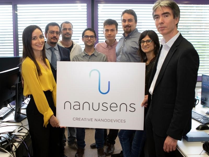
Some of the Nanusens team
The company has a solution for a major problem in the electronics industry -- namely that the production of key components, which are found in almost every electronic device, is limited by the current manufacturing methods. These are the sensors that are used to provide awareness to make them smart, as in smartphones, smart houses and smart cars. Called MEMS (Micro Electro Mechanical Systems), every design of sensor is unique and needs a specially developed production process to make it that can take up to seven years to perfect. This creates a problem as it is hard to ramp production and is the bottleneck preventing the MEMS market growing from billions to trillions of units a year.
Nanusens solves this by making MEMS sensors with the same standard production processes, called CMOS, that are used to make electronic chips in the giant production facilities, called fabs, around the world. Its unique approach builds sensor structures within the chip rather than on the surface as is done currently. This means that Nanusens can have its sensor chips made in any fab, in whatever volumes it requires, solving the volume production barrier of current MEMS products. This unlocks the MEMS market so that it can now grow to the trillions as has been predicted, especially with IoT, but so far has been unable to realise.
Moore's Law of electronics continually shrinking does not apply to MEMS as they have effectively hit a manufacturing barrier at around one micron. By using standard CMOS processes, Nanusens has smashed the MEMS shrinkage barrier and now NEMS can shrink in the same way as other electronic chips as they are now on the same shrinkage road map of CMOS. Nanusens is currently using 0.18 micron CMOS processes as this is a workhorse, fully debugged and supported node but sees no reason why smaller and smaller nodes cannot be used for future sensors.
The sensor designs made by Nanusens have another important advantage in that they are much smaller than current microscopic MEMS designs as they are on the nanoscale. This makes them NEMS (Nano Electro Mechanical Systems). The NEMS structures are built at the same time and on the same chip as the electronics needed to control them as the production processes are the same. Everything on one chip means that the final packaged solution is really tiny at only 1mm3. As conventional MEMS sensor packages each have to contain a chip for the control electronics and a chip for the larger MEMS structure, they are four times bigger at 4mm3. Each replacement with a Nanusens product means a saving of 3mm3. This will be even greater when Nanusens produce multiple sensors on one chip as the final packaged size hardly increases.

Using Nanusens nanosensors can free up space inside earbuds for larger batteries and more sensors
The first application where the space savings of these nanosensors will have a huge impact is earbuds. Freeing up space will enable larger batteries to be used solves the major issue of short operational life. The second challenge in earbuds is that designers want to have more sensors packed into the design to provide a better user experience with more features and better sound but are currently constrained by lack of available space. Nanusens' nanosensors enable many sensors to be designed in without taking up much additional space, and even less as multi-sensor solutions become available from Nanusens.
Similarly, wearables and smartphones can benefit from nanosensors but the biggest market is IoT (the Internet of Things). This has not taken off as predicted as MEMS sensors are not cheap enough, not small enough nor can they be made in the vast volumes needed. Nanusens solves all three of these problems so IoT can finally fulfil its potential of bringing awareness to everything, everywhere and unlock the MEMS market so that it can grow into trillions of units and trillions of dollars value.
"We have been in stealth mode for a number of years while we perfected and patent protected our technology to make nanosensors," explained Dr Josep Montanyà, CEO of Nanusens. "We launched at MWC2019 with the message that our nanosensors can help solve the issue of earbuds having short operational lives. This is because they are much smaller than current sensors and so free up room for larger batteries. This powerful message drew people in to learn more at the exhibition and a significant number of them then said that they wanted to invest in the company. We decided to open a new CrowdCube round as being the easiest way for more people to invest before our major Series A round that will be targeted to institutional investors towards the end of this year. The Series A round will be at a much higher valuation as we will have hit a number of key milestones on our journey to being a major new player in the MEMS sensors market and that will significantly enhance the value of the company."
Stuart Robinson, Director, Handset Component Technologies service at Strategy Analytics, added, "If MEMS isn't small enough for you then NEMS should be. Nanusens has taken MEMS technology to the next smaller level, developing nanoscale sensors inside the CMOS that can be integrated in the same silicon as the sensor controller. This is not a big deal for some applications but it's a game-changer for small devices that have multiple sensors such as accelerometers, gyroscopes, pressure and humidity sensors. Space-saving sensors leaves more room for other components such as a bigger battery. Every cubic millimetre counts in some devices so Nanusens is onto a winner here."
The UK has an excellent track record of high technology start-ups, particularly in the Electronics area, which is significantly helped by the British Enterprise Investment Scheme (EIS) scheme that incentivises investment in UK companies. The previous Nanusens CrowdCube round was oversubscribed once it came under the EIS scheme and then raised over a million Euros (£941,950).
The link to the Nanusens round on CrowdCube is www.crowdcube.com/nanusens
The video about the round is at https://vimeo.com/314458358
Background on Nanusens technology
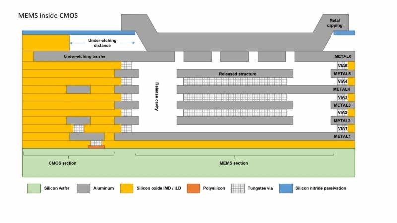
The Nanusens approach is to build MEMS sensors using the layer by layer, CMOS (Complementary Metal Oxide Semiconductor) process. Material (silicon dioxide) is etched away to release the mechanical structure that forms the MEMS. Although in this case, the MEMS structure is now ten times smaller than conventional MEMS making them NEMS.
In theory, this sounds very simple to do. In practice, it is very hard because the CMOS process was never designed for this purpose. The released metal structures have stresses and so distort rendering them useless. Nanusens has spent years researching and perfecting structure designs that do not distort when released. These, and variations thereof, are being patented to prevent others trying to copy Nanusens technology of NEMS-within-CMOS.

Nanusens shrink MEMS to create nanosensors within the CMOS layers