CyberOptics® Corporation, a leading global developer and manufacturer of high-precision 3D sensing technology solutions, will feature the WX3000™ metrology and inspection system with MRS™ sensor technology, and high-precision sensors for semiconductor tool set-up and diagnostics at the Virtual Connecting Heterogeneous Systems Summit Sept. 1-3, 2021.

Image Credit: CyberOptics Corporation
Tim Skunes, CyberOptics VP of R&D, will share a presentation ‘Improving Plating Uniformity for Hybrid Bonding and Micro Bumping,’ on Sept. 2nd at 8:50 a.m. ET/2:50 p.m. European CT.
Recent results have correlated copper thickness variations across a wafer during electrochemical deposition (ECD) to variations in metal dishing depth variations in hybrid bonding applications. Copper pillar coplanarity is also correlated to ECD plating uniformity in wafer bumping applications. The plating uniformity during ECD is directly affected by plating cell contact resistance. In-process monitoring of plating cell contact resistance can accurately predict when preventive maintenance is required to maintain thickness uniformity and save time and costs associated with test wafer measurements. A real-time sensor for measuring plating cell contact resistance will be presented.
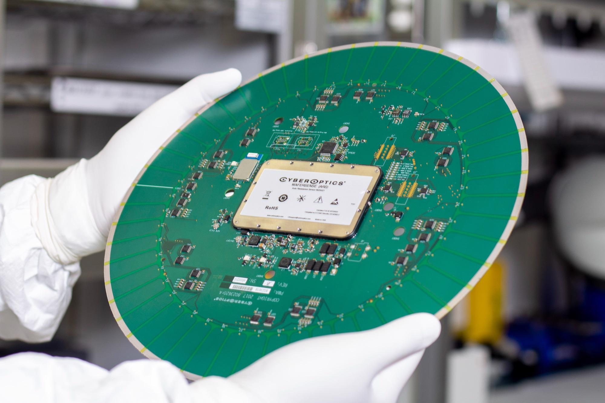
The company will virtually demonstrate high-precision sensors that process and equipment engineers use in the front-end of the fab to speed equipment qualification, shorten equipment maintenance cycles, lower equipment expenses and optimize preventative maintenance plans. The WaferSense® Auto Resistance Sensor™ (ARS) enables real-time resistance measurements of plating cell contacts in semiconductor Electrochemical Deposition (ECD) applications.
The company also will virtually showcase the 3 µm NanoResolution Multi-Reflection Suppression™ (MRS™) sensor integrated into CyberOptics’ WX3000™ system that provides sub-micrometer accuracy on features as small as 25µm. While retaining its ability to reject spurious multiple reflections, it adds the ability to capture and analyze specular reflections from shiny surfaces of solder balls, bumps and pillars, allowing highly accurate inspection and 3D metrology of these critical packaging features. Fast, complete 100% 3D/2D inspection and bump metrology can be conducted with throughput greater than 25 wafers (300mm) per hour.
“Fast, 100 percent metrology and inspection is needed now more than ever for wafer-level and advanced packaging applications,” said Dr. Subodh Kulkarni, President and CEO, CyberOptics. “Compared to alternative technologies, our systems are 2-3X faster with the high resolution and accuracy required to enable our customers to recognize significant improvements in yields and processes.”
The SEMI Connected Heterogeneous Systems Summit brings together thought leaders and industry experts from the entire 3D & Systems and packaging and, MEMS/imaging/sensor value chain to discuss the latest advancements in Heterogeneous Integration and sensing technology driving innovation in high end applications. CyberOptics is a gold sponsor.