Feb 14 2011
CMOS image sensors can now be used in a wide range of applications due to the breakthrough in the production method by the scientists at the Fraunhofer Institute of Microelectrical Circuits and Systems IMS, Duisburg.
Earlier, Spectroscopy was not possible using CMOS chips because of a coating, which made it impossible for UV rays to pass through them, like the image sensors used in multimedia electronics like cell phones or digital cameras. The coating of the CMOS devices with silicon nitride, a process called passivation formed a hard layer meant to protect the sensor from impurities, moisture and mechanical influences. The drawback of this process was that it limited the range of optical appliances since it does not allow the light in the UV and blue spectrum range to pass through, making the CMOS sensors color blind in high-performance applications like the automotive industry, which uses the optical semiconductor chips in driver assistance systems like road lane detection, blind-spot warning devices and parking aids.
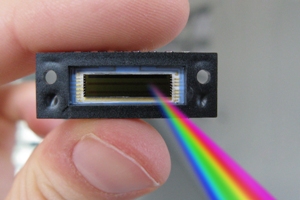
 CMOS Image Sensor
According to Werner Brockherde, who heads the department of Fraunhofer IMS, a new process allows for a protective coating, which allows the UV and blue light to pass through, while retaining the properties of the coating. This is achieved by increasing the nitrogen level in the coating due to which the absorption of shortwave light is reduced. This new transparent coating will thereby make it possible to use CMOS sensor in special applications where the sensors no longer have to cope with tough operating conditions like moisture and soaring temperatures, which make it inefficient while converting light into electrical signals.
With the modifications in the structure of the silicon nitride achieved by research scientists by altering the deposition parameters such as temperature and pressure, the protective layer becomes more sensitive to the blue and UV light, which according to Brockherde, makes the image detectors applicable for use in wavelength ranges down to 200 nanometers as opposed to 450 nanometers with standard passivation.
The CMOS image technology can now help laboratories across the globe by enhancing their accuracy and also provide scientists with images of greater detail with its application in professional microscopy.