Sep 18 2012
CMOSIS, the renowned European specialist for advanced CMOS image sensors, has developed a high-resolution, high-dynamic-range CMOS image sensor exclusively for Leica Camera AG geared to an important volume market.
The new “Leica M” digital camera launched at Photokina 2012 incorporates the full-custom CMOSIS “Leica MAX 24MP CMOS Sensor” featuring 24 Megapixels across an active sensor area of 36 x 24 mm², corresponding to the full-frame 35mm format. The sensor is the first milestone in a long term, strategic cooperation between Leica Camera AG and CMOSIS.
"This is the first time that a CMOS image sensor for a 35mm high-end camera was designed, and is manufactured, in Europe for a European customer," said Guy Meynants, CTO at CMOSIS, Antwerp, Belgium. "Apart from the ceramic IC package the Leica MAX 24MP CMOS Sensor is a 100-percent European product."
The new custom-designed sensor chip, counting 6,000 x 4,000 pixels on a 6 x 6 µm² grid across the active area of 36 x 24 mm², is made by STMicroelectronics (STM) in Grenoble, France, using 300mm wafers in their IMG175 CIS technology. STM's 110nm frontend and 90nm backend CIS technology with copper metallization was originally developed for CMOS image sensors with 1.75µm² pixels for mobile phones and other consumer applications. The large die size, larger than the reticle size, requires the use of one-dimensional stitching.
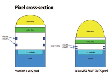
 Leica MAX 24MP CMOS Sensor - Pixel Cross-Section.
The imager for the “Leica M” is based on a 6 x 6 µm² pixel size, yielding a linear full well capacity of ≥40,000 electrons and a linear dynamic range close to 76dB. Pixel data are digitized by patented low-power, high-speed 14-bit column AD converters. The sensor features an electronic rolling shutter with global reset and noise cancellation through both analog as well as digital correlated double sampling (CDS) resulting in low temporal and spatial noise and non-uniformities.
Special care was taken in the sensor development to reduce crosstalk between neighboring pixels for a wide range of incident light angles. The sensor reduces spatial crosstalk by its very small distance between color filters and photodiodes. This thin optical stack is optimized for an efficient light coupling into the silicon. Microlenses with a strong curvature and high top height focus the incoming light rays in the center of each pixel's photodiode. The resulting low angular sensitivity of the quantum efficiency (QE) at high ray angles was achieved by the particular features of STM's 110/90nm CMOS process. This allows the “Leica M” to accept the full range of high-quality lenses in the camera system, which includes wide-angle, large aperture lenses, at their full optical performance.
Pixel size of 6x6 µm² and full frame rate of 5fps are state of the art and comparable to other high-end CMOS image sensors used in 35mm cameras. The 24MP CMOS sensor also allows Leica to offer, for the first time, full HDTV video recording and a live preview on an M-model camera. Power consumption of the sensor chip at full speed and resolution is specified at 700 mW. It is housed in a 78-pin ceramic package covered by a customized glass with anti-reflective coating and near-infrared cut-off filter.
“With CMOSIS, we are very pleased to have found a partner who made it possible for us to design and construct a sensor especially for Leica. Thanks to the special sensor technology and wide pixel aperture from CMOSIS, we can now, and for the first time, offer a digital system camera that is perfectly optimized for use with both M- and R-lenses”, said Alfred Schopf, Chairman of the Executive Board of Leica Camera AG. Leica is particularly proud of the fact that the “Leica M” employs a sensor “Made in Europe”, as a large proportion of the sensor is manufactured in France and Germany. “At the same time, the extremely low power consumption of the sensor brings added benefits for both image quality and battery life”, said Alfred Schopf.
About CMOSIS
CMOSIS is a pure-play supplier of standard off-the-shelf and application-specific CMOS image sensors for the industrial and professional market covering applications such as machine vision, high-end DSC markets, scientific, medical, automatic data capture and space. CMOSIS was founded in November 2007 as a fabless CMOS image sensor vendor providing in-house design, characterization, testing and qualification facilities for research, development and volume production. CMOSIS has developed unique IP related to CMOS image sensors such as global shutter pixels, fast and low-noise AD converters, backside illumination and increased dynamic range, resulting in six patents and several more pending. The company has grown continuously and consistently, currently employing more than 40 at its headquarters in Antwerp, Belgium.