Nov 30 2012
Leading semiconductor test equipment supplier Advantest Corporation has introduced the IC industry's fastest image-capture module to cost-efficiently test the high-frequency, low-power D-PHY and M-PHY interface chips expected to drive growth in the image sensor market. The new T2000 3Gbps CMOS Image Capture Module operates on Advantest's T2000 ISS system, an industry-leading test platform for a broad range of system-on-chip (SoC) devices.
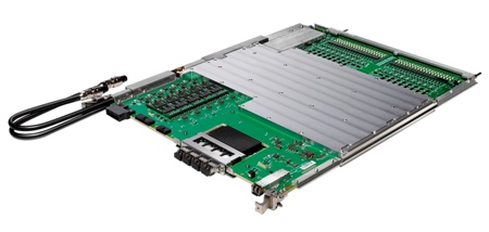
 Advantest T2000 ISS 3GICAP Module
With a high-speed image-capture rate of up to 3Gbps, Advantest's new 3GICAP test module performs highly accurate, massively parallel testing of CMOS image sensors, which are used in a wide range of consumer electronics, including cell phones, digital cameras, video camcorders and automotive vision systems.
"Ongoing, rapid improvements in the performance and resolution of CMOS image sensors as well as the growing volume of electronic products depending upon them continue to exert downward pressure on production costs," said Satoru Nagumo, senior vice president of the ASD Test Business Group at Advantest Corporation. "Our newest generation of image-capturing technology enables our customers to lower the cost of test while meeting the performance requirements for advanced image sensors."
The T2000 3Gbps CMOS Image Capture Module simultaneously tests up to 64 devices in parallel, significantly reducing test costs. In addition to improving yields by performing at-speed testing in production, the module also can be used to shorten turnaround time in verifying semiconductor designs on first silicon.
The new module is fully compatible with Advantest's T2000 ISS test platform, a member of the T2000 series. The T2000 family of test systems is used in the world's most advanced semiconductor design and production lines by integrated device manufacturers, fabless companies and outsourced semiconductor assembly and test foundries around the world.