Jun 22 2010
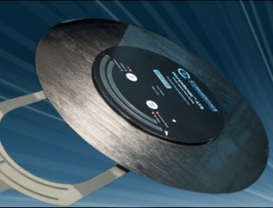
CyberOptics Semiconductor’s wafer gapping system, known as WaferSense AGS 300, has three capacitive distance sensors that can measure gaps that are vital to semiconductor processes’ outcome. Such processes include etch, sputtering, and thin-film deposition.
The AGS 300 can measure gaps between shower pedestals and heads at three different points. These points define a plane for ensuring reproducible and accurate equipment setups. The AGS 300 enables engineers to control the magnitude and uniformity of the gap better with high stability over a period of time.
 CyberOptics WaferSense
While legacy gap measurement techniques used crush blocks that were susceptible to variances of operator and instrument, and a wired leveling, the AGS 300 offers wireless-enabled measurements that have first film check rates at more than 99% accuracy.
AGS 300’s 7.5 mm height and wafer-like design permits automatic handling of maintenance, troubleshooting, and speed equipment set ups. Moreover, the wireless technique is repeatable and provides data to engineers for optimizing process controls and preventive maintenance schedules.
It will be possible to display data on a PC or laptop in real-time to enable quick gap adjustment and lower the tool calibration time. Existing measurements of gap are compared against the goals targeted, and gap tolerances are depicted in graphical and numerical formats to simplify adjustments. It will be possible to log the readings to enable setting up the same gap for all the tools, ensuring enhanced tool-to-tool processing uniformity.
The AGS300 is a component of WaferSense portfolio of devices from CyberOptics which include the Auto Teach System, Airborne Particle Sensor, Auto Vibration System and Auto Leveling System, with every device designed for optimizing wafer processing routines.