Jun 25 2010
SiOnyx Inc. demonstrated new pixel-scale detectors having a Detectivity (D*) of more than 1x10(14) Jones at room temperature. This demo, made possible by the join efforts of SiOnyx and the Army Research Office (ARO), showcases a 10x enhancement compared to conventional silicon detectors.
This breakthrough technique will empower SiOnyx to spearhead novel research programs along with the Defense Advanced Research Projects Agency (DARPA) and Army Night Vision and Electronic Sensors Directorate (NVESD) of the US Army.
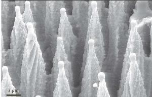
 Black Silicon under a Scanning Electron Microscope
SiOnyx is planning to commercialize a totally new semiconductor processing technique, which is an advanced method of development of cheaper, concise, and high-performing silicon photonic systems. SiOnyx's proprietary semiconductor process called the Black Silicon is based on a laser implant method pioneered at Harvard, and it improves the performance of light-sensing systems in applications across the industrial, consumer, defense, and medical industries. SiOnyx has demonstrated that this technology is applicable to CMOS image sensors and other photonic devices used in exacting applications in photodetection and imaging.
Following this milestone, SiOnyx is collaborating with the NVESD and DARPA of the US Army in research programs that focus on improving Black Silicon’s use in infrared imaging and low light.
The Director of NVESD, Dr. A. Fenner Milton, said that NVESD is concentrating on low light imaging, which can leverage silicon technology to bring down costs. The CEO of SiOnyx Stephen Saylor said that the basic features demonstrated by the company are responsible for the total quality of digital photography and medical imaging.
DARPA's Microsystems Technology Office Program Manager, Dr. Nibir Dhar noted that Black Silicon will enable the development of cheaper CMOS cameras for use in near-infrared systems.