Jun 29 2010
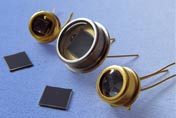
Semiconductor materials company, SiOnyx Inc., collaborating with the Army Research Office (ARO), demonstrated pixel-scale detectors featuring room temperature Detectivity (D*) that exceeded 1x10(14) Jones. In comparison with traditional silicon detectors, this pixel-scale detector represents 10x improvement.
This record for performance sets the trend to play a lead role in new sponsored research programs in conjunction with the Defense Advanced Research Projects Agency (DARPA) and Army Night Vision and Electronic Sensors Directorate (NVESD).

SiOnyx is on the path of commercializing a new technique for semiconductor processing, which is a breakthrough in the making of smaller, high performing, and cheaper silicon photonic devices. This technology is based on a unique laser implant method, commonly known as ‘Black Silicon’ that was primarily discovered at Harvard.
The SiOnyx patented semiconductor process, largely improves the performance of light-sensing devices in various industrial, medical, defense and consumer applications. The SiOnyx technology is also applicable in CMOS image sensors as well as other photonic devices mass-produced to meet the demands of photo-detecting and imaging applications.
According to the US Army NVESD's Director, Dr. A. Fenner Milton, NVESD is interested in imaging of low light level, which features the potential for capitalizing on silicon technology to lower costs.
CEO of SiOnyx, Stephen Saylor, states that the dynamic range and signal-to-noise ratio are features that dictate the any photonic system’s ultimate performance. In applications ranging from medical imaging to digital photography, these characteristics inspire experience quality. The groundbreaking results of SiOnyx’s work with ARO demonstrate a technology platform that can alter the industries’ performances.
Having completed this milestone, SiOnyx currently leads the DARPA and US Army's NVESD’s sponsored programs for advancing the utility of Black Silicon in infrared and low light imaging.