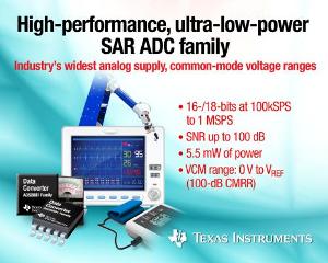
Texas Instruments (TI) today expanded its SAR (successive approximation register) analog-to-digital converter (ADC) product portfolio with a new family of 12 devices that provide the industry's widest analog supply and common-mode voltage ranges. The 1-channel ADS8881 family includes high-performance, ultra-low power 18- and 16-bit SAR ADCs with speed options ranging from 100 kSPS to 1 MSPS.
Engineers can chose the right ADC for their designs in a wide variety of applications – from high-end industrial, such as high-performance test and measurement equipment, precision metrology and precision sensor transmitters for industrial automation, to battery-operated test and measurement and portable medical. For more information about the ADS8881 family, visit www.ti.com/ads8881-pr.
 TI has added 12 high-performance, high-resolution, ultra-low-power SAR ADCs to product lineup. (PRNewsFoto/Texas Instruments)
Key benefits of the ADS8881 family:
- Widest input common mode: Most of the new ADCs provide an input common-mode range that is 20x wider than other devices. This simplifies signal conditioning and enables system designers to more easily digitize the difference between two independent sensor signals with widely varying common-mode voltage values over time.
- Flexible analog and digital supply voltage ranges: Features an analog supply voltage range of 2.7 V to 3.6 V, three times wider than existing devices. This enables direct operation from a Lithium-Ion battery. Also, with an even wider digital supply voltage range of 1.65 V to 3.6 V, the ADCs meet most microprocessor supply requirements.
- Ultra-low power: The 1-MSPS SAR ADCs consume only 5.5 mW of power at 1 MSPS and 55 uW at 10 kSPS, making them suitable for pulsed DC measurements in portable medical and heat-sensitive automated test applications.
- Large pin-compatible family: All 12 devices are pin-compatible and available in both MSOP and QFN package options, enabling engineers to reuse the same analog signal chain design across their products with minimal, if any, redesign.
Tools and support to jump-start design
TI offers a range of support tools for the ADS8881 family to speed time to market, including reference designs, simulation models and hardware evaluation kits.
The following TI Precision Designs reference design circuits provide theory, simulation, calculation, design methodology and more.
- Multiplexed and step-response:
- Data Acquisition for MUX and Step Inputs, 18 bits, 1 uS Full-Scale Response
- 16-bit, 400-kSPS, 4-Ch. Multiplexed Data Acquisition System for High-Voltage Inputs
- High precision:
- Data Acquisition Optimized for Lowest Distortion, Lowest Noise, 18 bit, 1Msps
- Low power:
- Data Acquisition at 1 KHz AC, 1 mW, 18 bit, 1 Msps
- Data Acquisition for 10 kHz AC, 35mW, 18 bit, 1 Msps
- Medical:
- Data Acquisition Block for ECG Systems, Discrete LEAD/ECG Implementation
The ADS8881EVM-PDK, ADS8861EVM-PDK and ADS8860EVM-PDK performance development kits may be purchased for US$199. The kits enable system designers to quickly evaluate and test device performance using only the provided hardware and TI's ADCPro™ software tool.
IBIS and TINA-TI™ models are also available for the ADS8881 family to optimize front-end signal conditioning circuitry in software simulation.
Support is available on the Precision Converters Forum in the TI E2E™ Community, where engineers can search for solutions, get help, share knowledge and solve problems with fellow engineers and TI experts.