Oct 10 2014
Optical emission spectrometers are widely used in the steel industry but the instruments currently employed are relatively large and bulky. A novel sensor makes it possible to significantly reduce their size and, moreover, enables a more precise analysis in half the time previously required.
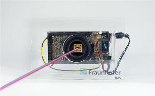
 Emission spectrometers analyze materials on the basis of their emitted light spectrum. Novel sensors permit the development of even smaller, faster and more precise test instruments. (© Fraunhofer IMS)
Gold is expensive, so it is only natural that jewelry buyers should want assurance that the precious ring or necklace they have set their heart on is really made of genuine gold. Jewelers in India are required by law to test the purity of gold using an optical emission spectrometer that analyzes the composition of the metal on the basis of the emitted light spectrum. But goldsmiths are not the only users of these instruments; the tools are more frequently found in steel foundries and car factories where they help engineers to determine the characteristics of steel materials, analyze their chemical composition, and assess their quality. Until now, this involved using very bulky equipment, at least in applications requiring a high resolution.
Researchers at the Fraunhofer Institute for Microelectronic Circuits and Systems IMS in Duisburg have developed a sensor that shrinks the size of the spectrometer optics. “Whereas earlier high-resolution spectrometers were the size of a washing machine, those built using our sensor will be no bigger than a microwave oven,” says IMS department head Werner Brockherde. And this is not the only advantage of the new sensor: the delivered results are also more precise and available in half the time. This can be beneficial, for example, when performing quality assurance in the automotive industry.
The first sensor that combines time- and space-resolved measurements
To understand how the scientists were able to miniaturize the instrument to this extent, we need to take a closer look at its inner workings. In order to analyze a piece of steel, for example, it has to generate sparks at regular intervals. These sparks knock atoms out of the material, resulting in a plasma that emits multicolored light. The plasma light is split into two beam channels and broken down into several wavebands, like the colors of a rainbow, which are then analyzed separately. In the first beam channel, light-sensitive electronic components known as CCD line sensors record the entire spectrum of the sample. This reveals the nature and concentration of particles suspended in the plasma, from which it is possible to derive information on the composition of the steel sample. Experts refer to this result as a space-resolved measurement. The second beam channel produces time-resolved measurements of individual spectral lines – adjusted so that the instrument can distinguish between light emitted by te plasma and that emitted by the sparks. All previous solutions were based on separate time-resolved and space-resolved measurements. “Our CMOS-based sensor enables these two sets of measurements to be conducted in parallel. As a result, we only require a single beam channel and thus a single optical unit,” says Brockherde.
The new photo-detector multiplies the dynamic range by 100, resulting in a much faster spectrometer. It is capable of measuring signals in the microvolt range at the same time as signals measuring some 100 millivolts. Until now, this required several measurement cycles. As well as increasing measurement speed, the high dynamic range also offers other advantages. “Because we can now measure the entire spectrum with a single series of pulses, the measurement accuracy is also higher,” reports Brockherde.
Demonstrator at the Vision trade show
A demonstration version of the sensor will be presented at the Vision trade show in Stuttgart from November 4 to 6 (Booth 1H74). An evaluation kit for interested design engineers is also available. “The market for spectroscopy equipment is dominated by German manufacturers,” says the scientist. “Our new sensor, which was developed in Germany and is not available anywhere else, will enable these manufacturers to secure a further competitive advantage.”