Dec 22 2015
Making an incredibly fast photodetector is one thing, but actually measuring its speed is another.
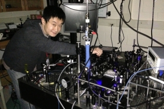
 Haining Wang in his lab. Credit: Provided
Graduate student Haining Wang came up with an inventive way of measuring the near-instantaneous electrical current generated using a light detector that he and a team of Cornell engineers made using an atomically thin material.
The team, headed by Farhan Rana, associate professor in the School of Electrical and Computer Engineering, measured the ultrafast response of their two-dimensional photodetector using a strobe-like process called two-pulse photovoltage correlation.
The team’s paper, “Ultrafast response of monolayer molybdenum disulfide photodetectors,” was published in Nature Communications, Nov. 17.
“It was very clever,” Rana said of Wang’s idea. “He came up with this idea of essentially hitting the device with an optical pulse [to initiate an electrical charge] and after a small delay, hitting it with the pulse again. By varying the time between the first and second pulse, and looking at the response of the device as a result, you can sort of see what the intrinsic speed of the device is.”
Rana’s team used a 3-atoms-thick sheet of molybdenum disulfide (MoS2), a material Rana and others have tested previously in photodetection studies. Photodetection is used in various high-speed optoelectronic applications, including optical fiber networks.
According to Wang’s experimentation, the MoS2 photodetector had intrinsic response times as short as 3 picoseconds; a picosecond is one-trillionth of a second. Co-author Wang said the speed at which the MoS2 detector responds is vastly superior to current technology, and is partly due to the extremely short distance the charges generated by light must travel before making it out of the device and into the external electrical circuit.
“State-of-the-art optical communication links work at around 10 GHz per channel, so if you make 10 channels in parallel, you have a 100 GHz optical communication link,” he said. “We find that this single device can work up to 300 GHz, which is an amazing speed.”
Wang also said that, despite being just 3-atoms thick, MoS2 is “extremely easy to make” and relatively inexpensive, adding to its appeal.
As with all photodetectors, however, the downside is the low quantum efficiency, which is a measure of the number of charges generated by the detector in the external circuit per incident photon.
In the Rana team’s work, only a small percentage of the light-generated charges – 1 to 2 percent – were able to escape the photodetector and make it into the external circuit; most recombined inside the device, producing heat. Market-available photodetector materials such as silicon and gallium arsenide, while generally much slower, have efficiencies of anywhere from 50 to 90 percent.
“That’s the tradeoff of these devices,” Rana said. “Every photodetector ever made has always had to face the efficiency-speed tradeoff.”
Further research by the group will include a discovery made by both Rana’s team and a research group at the University of California, Berkeley: coating the sample with a chemical that will “basically kill the recombination completely,” Rana said.
“So you have to play around with these material surfaces and make sure you’re attaching the right molecules and atoms to it on the outside,” Rana said.
The Berkeley group reported in November an efficiency of 95 percent using their chemically coated MoS2 photodetector.
Rana said the photodetection technology will play a major role in emerging fields, such as LiFi – using light as a source of wireless communication. He said windows and walls could be coated with atomically thin layers of material that would interact with light and carry Internet signals.
Other co-authors include former graduate students Changjian Zhang and Weimin Chan, and Sandip Tiwari, the Charles N. Mellowes Professor of Engineering.
Their research was supported by the Cornell Center for Materials Research, under a National Science Foundation grant, the Air Force Office of Scientific Research, the Office of Naval Research, as well as an NSF grant to the Cornell NanoScale Science and Technology Facility.