Feb 11 2019
A KAIST study team created a silicon optical phased array (OPA) chip, which can be a key component for 3D image sensors. This study was co-led by PhD candidate Seong-Hwan Kim and Dr. Jong-Bum You from the National Nanofab Center (NNFC).
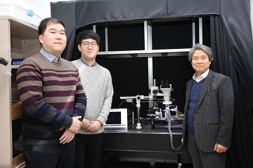
 From left: Dr. Jong-Bum Yo, PhD candidate Seong-Hwan Kimand Professor Hyo-Hoon Park. (Image credit: KAIST)
A 3D image sensor integrates distance information to a 2D image, such as a photo, to identify it as a 3D image. It plays an important role in many electronics including autonomous vehicles, robots, drones, and facial recognition systems, which necessitate correct measurement of the distance from objects.
A number of drone and automobile companies are concentrating on creating 3D image sensor systems, based on mechanical light detection and ranging (LiDAR) systems. But, it can only be made as small as the size of a fist and has a high chance of not working as it employs a mechanical technique for laser beam-steering.
OPAs have garnered a lot of attention as a core component to execute solid-state LiDAR as it can regulate the light direction electronically without moving parts. Silicon-based OPAs are small, hard-wearing, and can be mass-manufactured via conventional Si-CMOS processes.
However, in the progress of OPAs, a big problem has been highlighted about how to realize broad beam-steering in longitudinal and transversal directions. In the transversal direction, a broad beam-steering has been executed, fairly easily, through an electro-optic or thermo-optic control of the phase shifters integrated with a 1D array. But the longitudinal beam-steering is still a technical challenge as only a narrow steering was achievable with the same 1D array by altering the wavelengths of light, which is difficult to execute in semiconductor processes.
If a light wavelength is altered, features of element devices containing the OPA can differ, which makes it hard to regulate the light direction with dependability as well as to incorporate a wavelength-tunable laser on a silicon-based chip. Thus, it is vital to plan a new structure that can simply regulate the radiated light in both longitudinal and transversal directions.
By incorporating tunable radiator, rather than a tunable laser in a conventional OPA, Professor Hyo-Hoon Park from the School of Electrical Engineering and his team built an ultra-small, low-power OPA chip that enables a wide 2D beam-steering using a monochromatic light source.
This OPA structure enables reducing the size of 3D image sensors to as small as a dragonfly’s eye.
According to the researchers, the OPA can work as a 3D image sensor and also as a wireless transmitter transmitting the image data to a preferred direction, allowing high-quality image data to be spontaneously communicated between electronic devices.
It’s not an easy task to integrate a tunable light source in the OPA structures of previous works. We hope our research proposing a tunable radiator makes a big step towards commercializing OPAs.
Seong-Hwan Kim, PhD Candidate, National Nanofab Center, KAIST
We will be able to support application researches of 3D image sensors, especially for facial recognition with smartphones and augmented reality services. We will try to prepare a processing platform in NNFC that provides core technologies of the 3D image sensor fabrication.
Dr. Jong-Bum You, National Nanofab Center, KAIST
This study was reported in Optics Letters on January 15th.