Jun 3 2010
A new technique to realize in-chip multi-sensors solution akin to the build up of receptors for living organisms has been suggested by the Institute of Control and System Research (ICSR)-Bulgarian Academy of Sciences (BAS) scientists.
Presently it is possible to use nano or micro sensors to measure more than one parameter of non-electrical entities simultaneously. Separate converting zones are created in silicon or any other substrate for realizing such measurements. This helps in converting non-electrical parameters like pressure, magnetic field, light, temperature and so on, to electrical signals. However, it is difficult to realize such a solution in a chip that requires a complicated integral format having many condensers, resistors, transistors, transistors, diodes, etc in a chip. A large number of connections, contacts, electromagnetic compatibility, physical restrictions and masks are the other limiting factors.
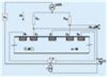
 BAS multi sensor for magnetic field, temperature and light
A novel technique suggested by the ICSR-BAS scientists relates to realizing a practical in-chip solution analogous to the process of build up of receptors inside living organisms. Such a functional principle is applied in the sensor electronics field wherein the physical phenomenon along with the effects of the phenomenon exist together within a single region in a structure of a solid semiconductor. Such a technical solution is able to overcome most of the drawbacks of discrete multi-sensors.
National business representatives participated at the BAS scientists’ first innovation meeting on 15 June, 2009, when technology transfer ready innovations were examined and attracted industry interest to the development of the functional silicon multi-sensor. The solution’s positive result that was not expected is a reaction to innovations posed by the project scientists. These questions related to the hidden element in the arbitrary sensor’s zone, the feasibility of using signal processing to get metrological information or the creation of an extra contact for the arbitrary sensor’s zone, and the type of parallel mechanisms in the zone. However, this unique technique forms the core of the functional multiple sensors for light, temperature, magnetic field, three dimensional and two dimensional vectors with exceptional resolution.
Customary silicon integrated technology is utilized to realize the functional multisensor. The linear functional multisensor structure is able to extract the sensor signals using just five contacts and a scheme that is simplified to the maximum. This invention has combined the Lorenz force, a reverse-biased photodiode’s behavior and a forward-biased diode’s temperature dependency in current source mode.
The Bulgarian Chamber of Industry and Commerce’s representative has termed the functional multi-sensor used for light, temperature and magnetic field as ‘sensor 3 in 1,’ a humorous name. Its exceptional sensitivity results and performance achieved render it fit for technological transfer.